The thumbnail is the reduced image of the PCB tested by the current AOI equipment, which is convenient for global observation, display of error positions and other related operations. At the same time, if people want the camera to move to a certain position, they only need to double-click the corresponding position on the thumbnail.
Production method: After completing the operation of the new program menu bar, click OK, the system will automatically prompt “Are people making PCB thumbnails now?” Click “Yes”, the system will calculate the starting point and size according to the set PCB Scan the thumbnail of the PCB. Or directly click on the “make board map” in the lower right corner of the main window, as shown in the figure:
In order to allow the thumbnail to display the PCB completely, people can select an appropriate reduction ratio. Generally, the thumbnail window can display the outline image of the entire PCB. Click “Full image” to automatically expand the PCB thumbnail according to the window screen size. The thumbnails achieve the best display effect. The method of making offline AOI equipment diagrams is similar to that of making thumbnails (just select the location and file name to save the image). The offline AOI equipment diagram can be used on other computers (not the computer on this equipment) to compile test programs (the use method is similar to the equipment use method).
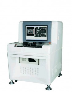
PCB under AOI detector
Note: Offline AOI device programming is an optional function, if necessary, please purchase it separately.
1.7 Set MARK point
Generally choose two easily identifiable points on the diagonal of the PCB as the MARK point, which can be the MARK point on the PCB itself, or the fixed hole on the board as the MARK point.
Note: 1. When the MARK point on the PCB is often oxidized, try to use the upper hole position as the MARK point, because AOI equipment is more sensitive to color changes, and a slight change may cause MARK recognition errors. The color changes of bits are generally relatively small. (Figure 1)
2. When setting the MARK point, do not select the point with similar images in the nearby position, so as to avoid searching error and cause the positioning frame to be completely offset. (Figure 2)
“As shown in the figure: After selecting OK, the camera will automatically move to the lower left corner of the detection area (usually MARK is in the lower left-upper right area), people can click the arrow keys on the operation window to move the camera to the position of the MARK point on the PCB board, Or directly click the corresponding position on the thumbnail.
As shown in the figure, a MARK point positioning box and MARK will appear on the main window interface.
When doing MARK, try to use circular MARK as possible.
When it is found that a board cannot pass the MARK point calibration during the test (the fixture will automatically spring back to the loading point during testing), observe the reason, if it is the position of the MARK positioning frame It is correct, but the error value is too large to pass. People can properly adjust the error range of the MARK point to make the MARK correction pass. Note that the maximum error range of the MARK cannot exceed 25%; if the position of the MARK positioning frame is wrong (when the AOI equipment detects, the fixture will Automatically bounce back to the loading point), that is, when the correct MARK position cannot be searched, the search range of the MARK can be adjusted appropriately, and the maximum cannot exceed 5mm. If the MARK recognition sensitivity is not enough (there are obvious MARK recognition errors, but the error is not high), people can select the “maximum” and “visual” options in the grayscale processing or adjust the contrast to increase the sensitivity.
Media Contact
Company Name: EKTION (SHENZHEN) TECHNOLOGY LIMITED
Email: Send Email
Phone: +86-755-27321258
Country: China
Website: https://www.aoiekt.com/
